
Understand CMOS Image Sensors! Definition And Overview Of “Sensor”
Sales Engineer:Grace Gao
Email:grace@bri-elec.com
WhatsApp:0086-199 2997 5286
At present, except for some special fields, CMOS image sensors occupy the vast majority of the market. Today, we will briefly introduce some basic concepts and noun concepts of CMOS image sensors.
1. What is a CMOS image sensor?
CMOS (Complementary Metal Oxide Semiconductor), which is a complementary metal oxide semiconductor, is a semiconductor that can record changes in light. It mainly uses semiconductors made of silicon and germanium, so that N-type and P-type semiconductors coexist on CMOS. This The current generated by the two complementary effects can be recorded and interpreted by the processing chip as an image.
CMOS image sensor (CMOS imager Sensor), referred to as CIS, is an image sensor using CMOS technology, an image sensing element manufactured using the principle of photoelectric technology.
2.Pixel
Pixel is the smallest photosensitive unit of the image sensor. The pixel array is arranged together to form the photosensitive area of the image sensor.
Pixel Size refers to the size of a single photosensitive element of the image sensor. Generally, we can see two expressions, such as 1.12μm or 1.12μm×1.12μm. The larger the size of the pixel, the more photons it receives and the more charge it generates under the same lighting conditions and exposure time.
Effective pixels (Number of effective pixels) refer to the pixels in the CIS that can perform effective photoelectric conversion and output image signals. It is an important technical indicator for measuring CIS. For example, Sony's classic CIS - IMX586, has an effective pixel of 8000 (H) × 6000 (V), which means that the number of horizontal pixels is 8000 and the number of vertical pixels is 6000. Multiplying the two numbers is 48 million, also known as 48M Or 48MP. M and MP are the abbreviations of Megapixel.
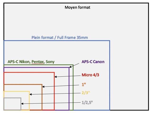
3.Optical size/target surface size
We often see that the Sensor is a fraction of a point, which refers to the size of the CMOS image sensor. This size refers to the target surface size of the sensor, mainly by calculating the diagonal length of the sensor target surface, and then Convert it to inches, such as the common 1 inch (1"), 1/2 inch (1/2"), 1/4 inch (1/4"), etc.
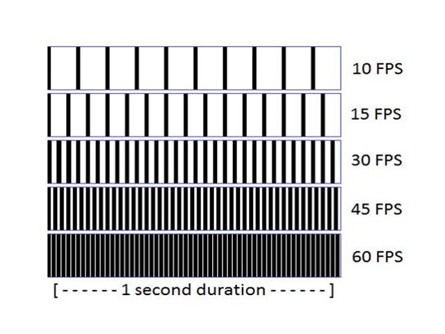
4.Frame rate
Frame rate (Frame Rate) represents the number of pictures recorded or played per unit time. The frame rate per second represents the number of times the graphics sensor can update per second when processing the field. The higher the number of frames, the smoother the picture displayed.
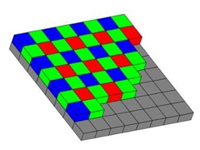
5.CFA
CFA (Color Filter Array), that is, color filter array. Since CIS itself cannot sense the wavelength of light, that is, it cannot sense color. The function of CFA is to allow CIS to sense color. Currently, the mainstream uses Bayer array, also known as RGGB or RGB Bayer. The sensor form without CFA is called monochrome (MONO), which is a black and white sensor. The MONO sensor has a more delicate layer transition and a higher signal-to-noise ratio.
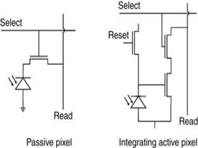
6.Pixel Type/Pixel Technology
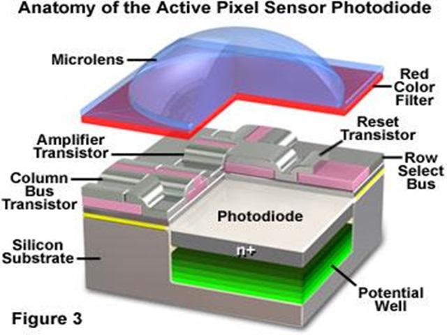
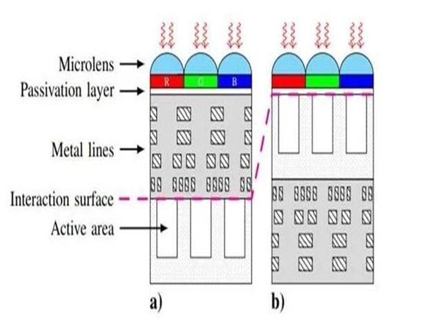
Mainly divided into two types: FSI (front-illuminated) and BSI (back-illuminated). The metal wiring layer of the front-illuminated type is between the CFA and the photodiode. When the light enters the diode, there will be loss. The back-illuminated type uses the metal wiring layer. The layer is placed under the photodiode, and the light can directly enter the photodiode after passing through the color filter. This structure not only increases the amount of light, but also effectively suppresses the decrease in sensitivity caused by changes in the incident angle of the light. Today, back-illuminated has become the mainstream technology for mid- to high-end CIS. Stacked/Stacked (Stark) is an improvement on the back-illuminated type. It moves the circuit layer to the bottom of the photosensitive element, maximizing the photosensitive area and reducing the overall area of the chip.
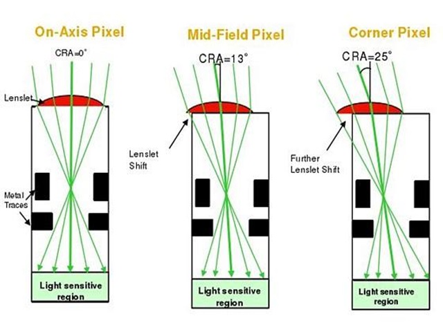
7.CRA Angle
CRA angle: From the sensor side of the lens, the maximum angle at which light can be focused onto the pixel is defined as the Chief Ray Angle (CRA), also called the chief ray incident angle. The lens axis is close to zero degrees, and the greater the distance from the axis, the greater the angle. CRA is related to the position of the pixel on the sensor. If the CRA of the lens is smaller than the CRA of the sensor, there will definitely be a color cast.
8.Transmission interface
There are mainly interfaces such as MIPI and DVP. (Mobile Industry Processor Interface) is a serial port and a mobile industry processor interface. It is an open standard for mobile application processors initiated by the MIPI Alliance. It has the characteristics of fast transmission speed and strong anti-interference ability. There are mainly CLKP/N and DATAP/N pins, generally 1/2/4Lane. DVP (Digital Video Port) is a parallel port, which mainly has MCLK, PCLK, VSYNC, HSYNC, and DATA pins. It can transmit 8/10/12 bits data, but the speed is slow and the transmission bandwidth is low.
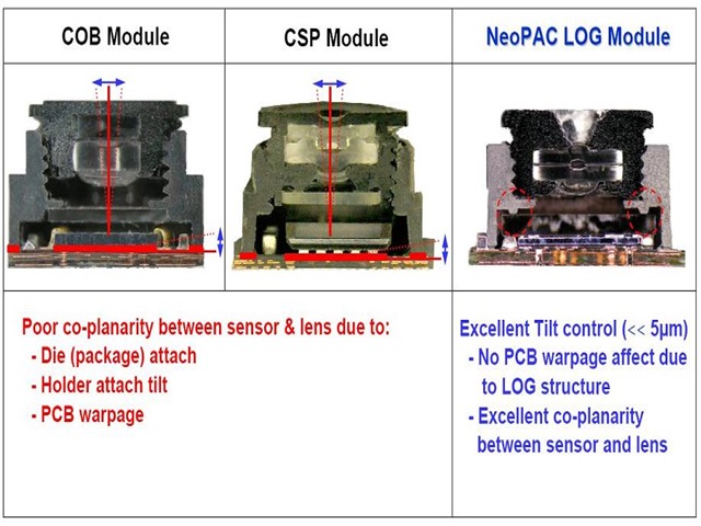
9.Package
Package, CIS packaging mainly includes COB, CSP, PLCC, BGA, LGA, PGA and other packaging methods. COB (chip on board) refers to the technology that directly connects the bare chip to the PCB. That is, the bare chip connects the signals on the chip and the circuit board together through wiring. It is also called top packaging technology, CSP (Chip Scale). Package) package, that is, chip-scale packaging, is a package product developed on the basis of BGA and is very close to the chip size. It has the characteristics of small size, good electrical performance and excellent heat dissipation.
PLCC is to print CIS onto the substrate through the COB process, then cover the bracket and attach IR to become PLCC. The bottom four sides of the PLCC contain soldering pads, so that the PLCC can be mounted on the FPC through SMT. After SMT, the motor and lens can be assembled to make a camera module.
BGA is a spherical contact arrangement and surface mount package. LGA is a planar grid array package, while PGA is a pin grid array package.
CMOS is the abbreviation of Complementary Metal Oxide Semiconductor. It refers to a technology used to manufacture large-scale integrated circuit chips or a chip manufactured using this technology. It is a readable and writable RAM chip on the computer motherboard. Because of its readable and writable characteristics, it is used on the computer motherboard to save the data after the BIOS sets the computer hardware parameters. This chip is only used to store data. A voltage-controlled amplifier device is the basic unit of a CMOS digital integrated circuit. The setting of various parameters in the BIOS requires special procedures. The BIOS setup program is generally integrated into the chip by the manufacturer. You can enter the BIOS setup program by pressing specific buttons when turning on the computer, making it easy to set up the system. Therefore BIOS settings are sometimes called CMOS settings.
In the field of digital imaging, CMOS was developed as a low-cost photosensitive element technology. The photosensitive elements of common digital products on the market are mainly CCD or CMOS, especially low-end camera products, and usually high-end cameras are CCD Photosensitive element.
Sales Engineer:Grace Gao
Email:grace@bri-elec.com
WhatsApp:0086-199 2997 5286